PROJECTS
PDF Fingerprint ID System
System Overview
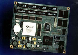
The new design was significantly different from the original implementation. The DSP was mounted in a Ball Grid Array (BGA) package and provided no debug access. To facilitate debug, Bolton Engineering implemented the prototype system on a slightly wider board, placing logic analyzer headers outside the active area. Once debug was complete, the headers were removed to restore the board to the desired size.
- 1.6 billion operations per second computational capacity.
- Implemented low-power CCD camera electronics on separate flexible circuit card (not shown).
- Designed frame grabber using Intel/Altera MAX-series Programmable Logic Device (PLD) and DSP DMA.
- Incorporated wide operating range multi-voltage high-efficiency synchronous power supply.
- 16 megabytes of industry standard sector-programmable FLASH memory.
- 8 megabytes of fast EDO DRAM.
- Four serial ports: one TTL-level, one RS-485, two RS-232.
- Battery backed up real time clock.
- Full test point access.
- Designed to meet FCC part 15 class B, EN 55022 class B.
Results
- Product delivered on time, for industry trade show.
- Electronics met or exceeded all design goals, and came in at budgeted cost.
Project Scope
Bolton Engineering was responsible for writing the specification, designing and simulating the PLD logic, creating schematics, laying out the circuit board layout, writing test software, testing, and writing documentation.

Bolton Engineering, Inc. had designed the client’s first generation Fingerprint ID System using a quad-processor DSP. The client wanted to move to a less expensive dual-processor DSP, increase fingerprint template capacity and add I/O. The unit had to fit into the same case with similar power requirements.


